Endura 5500

Overview
Product sourcing insights & recommendations


The phrase "Endura 5500" refers to the Applied Materials (AMAT) Endura 5500, widely recognized as the most successful metallization system in semiconductor history Chiphistory. Originally launched in July 1990, it revolutionized the industry as the first "bullet-proof" multi-chamber platform, enabling wafers to pass through multiple deposition steps without breaking vacuum ChiphistoryChinsortech.
Product Overview
The Endura 5500 is a modular PVD (Physical Vapor Deposition) platform designed primarily for 150mm (6-inch) and 200mm (8-inch) wafers BridgetronicBroadwayengineering.
* Modular Architecture: It features a monolithic multi-cavity design supporting up to nine process chambers, allowing for high-productivity sequences like degas, pre-clean, and multi-layer metal deposition (e.g., Al, Ti, TiN, TiW, and W) BroadwayengineeringChinsortech.
* Robotics & Throughput: Equipped with HP, HP+, or VHP (Very High Productivity) robots, the system is engineered for maximum uptime and reliability BroadwayengineeringMacquarie.
* Technological Impact: Over 4,500 systems were shipped within its first two decades, processing the vast majority of integrated circuits manufactured during that era Chiphistory.
Market Trends & Insights (2025–2026)
Despite its age, the Endura 5500 is currently experiencing a major resurgence due to the growth of Legacy Fabs and the "More-than-Moore" (MtM) sectors .
* 200mm Fab Expansion: Global 200mm fab capacity is projected to reach a record high by 2026, driven by a 14% growth rate in sectors like automotive, power electronics, and IoT .
* Demand for Refurbished Systems: There is an intense secondary market for refurbished Endura 5500 units. Legacy fabs (producing chips at 180nm to 65nm) prefer these systems for their lower capital expenditure and proven reliability compared to newer 300mm alternatives .
* Power & EV Growth: The shift toward Electric Vehicles (EVs) has spiked demand for Power MOSFETs and IGBTs. The Endura platform has been adapted to handle new materials like Silicon Carbide (SiC) and Gallium Nitride (GaN), often featuring specialized handling for fragile, transparent substrates .
* Spare Parts Economy: A robust "2nd source" market exists for components like chamber liners, electrostatic chucks (ESCs), and robotic arms, as fabs seek to extend the life of their existing Endura fleets SemiconserviceChinsortech.
Market Outlook Summary
| Metric | 2025-2026 Outlook |
|---|---|
| Market Segment | ICAPS (Image Sensors, Comms, Automotive, Power, Sensors) |
| Regional Driver | Led by China, followed by SE Asia and the Americas |
| Secondary Market | High demand for "Certified Refurbished" and upgraded legacy tools |
| Material Innovation | New support for ScAlN (RF filters) and PZT (MEMS) |
Based on the market resurgence of legacy nodes, would you like to:
Semiconductor Fabrication Equipment Pvd 200mm Refurbished
Products · Top picks & verified manufacturers
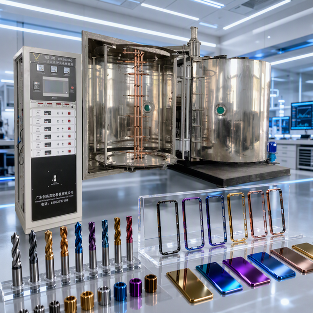
Pvd Coating Equipment High Efficiency Watch Coating Best Selling Automatic Cost Effective Precision Easy Operation
 Guangdong Chuanggao Vacuum Technology Co., Ltd.verified🇨🇳CN2 yrs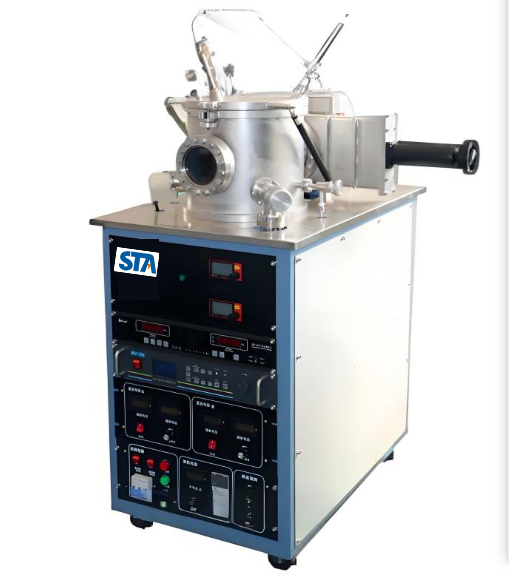
Factory Price High Temperature Thin Film Deposition Magnetron Sputtering Coating System PVD Coating Equipment
 Sta Refractory (zhengzhou) Co., Ltd.🇨🇳CN14 yrs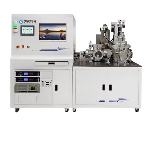
Low-temperature Annealing Magnetron Sputtering Equipment PVD Lab High Accuracy Physical Vapor Deposition Coating Equipment Motor
 Anhui Ancourage Scientific Co., Ltd.🇨🇳CN4 yrs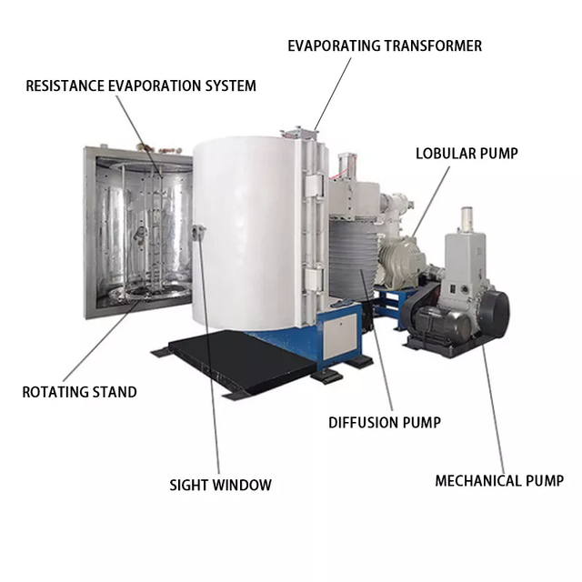
Factory China-based PVD Coating Machine Chrome Spray Plating Machine Vacuum Equipment for Jewelry Christmas Decorations
 Shaanxi Longstar New Material Technology Co., Ltd.🇨🇳CN6 yrs
Factory China-based PVD Coating Machine Chrome Spray Plating Machine Vacuum Equipment for Jewelry Christmas Decorations
Related Searches
Explore more sourcing topics & related categories
Sources & References
25 sources cited · Verified industry data & reports
AMAT Endura 5500
eBay
Silver AMAT Endura 5500 with complex wiring and heat sinks on green factory floor. Black AMAT Endura 5500 with white panels, exposed engine, and dual side ports ...
AMAT / APPLIED MATERIALS Endura 5500 Reactor used ...
CAEOnline
AKT/AMAT / APPLIED MATERIALS / AKT Endura 5500 is an advanced PECVD (plasma enhanced chemical vapor deposition) reactor that offers maximum productivity, ...

Applied Materials - Endura 5500 PVD
Chip History
Summary : Applied Materials - Endura 5500 PVD: The first bullet-proof multi-chamber, multi-process system. It would become the most successful metallization ...

Endura 5500 | Products | Broadway Engineering
broadwayengineering.com
Broadway Engineering can supply many configurations of the Endura 5500, Centura 5200 / 5300 and P5000. These systems include installation and warranty.
Manufacturing evaluation of an Endura 5500 PVD ... - Gale
gale.com
The Endura 5500 PVD system is based on a multichamber, staged-vacuum architecture [2]. Figure 1 shows the basic configuration: two isolated cassette ...

Applied Materials (AMAT) Endura 5500 Liner/Barrier
Macquarie
Pumps, chillers, and support items may not be included, please inspect the tool to confirm. Endura 5500. VHP Robot. 2 CVD / 3 PVD Chambers: 2TxZ/1Ti/1IMP Ti/1Co.